Research
Creation of Si atomic-layer ribbons by self-assembled wet fabrication
It is known that when materials are reduced in dimension to the nanometer range, they exhibit unique properties that are not observed in bulk (large mass). The key to next-generation electronic and optical devices is the active incorporation of nanomaterials that demonstrate these quantum mechanical effects. We are endeavoring to develop a new method to create "ribbons" of Si atomic layers with controlled "width" and "thickness".
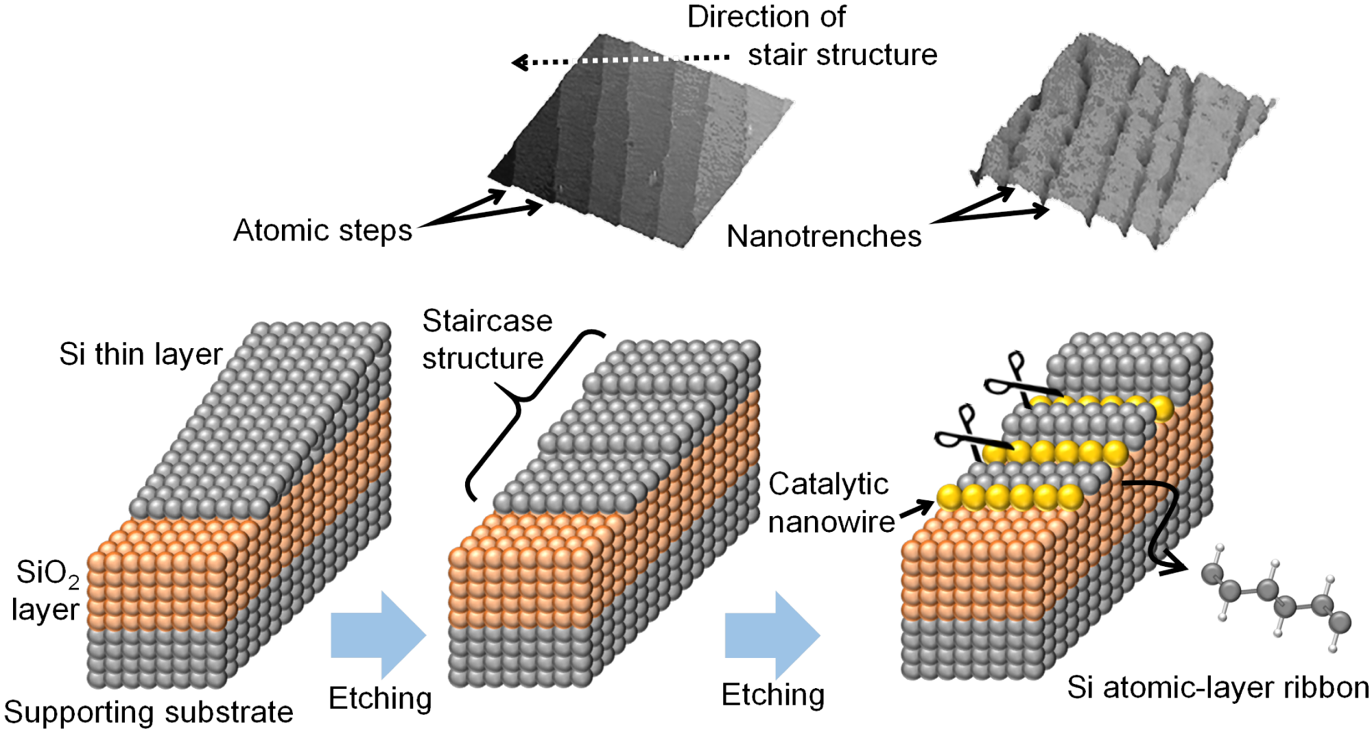
Cutting of Si atomic-layer ribbons from Si crystal
Atomic-scale performance evaluation of "surface creation processes"
In the field of "manufacturing," we engage in studies and technologies related to "creating the form and function of solid surfaces as desired." To enhance the performance of surface creation processes, measurement technology for evaluating them is indispensable. We visualize semiconductor surfaces precisely treated in an ultra-clean environment using microscopes with atomic-level resolution. This enables us to evaluate the performance of various practical processes (such as ultra-precision machining, wet cleaning, film formation, etc.) on an atomic scale.
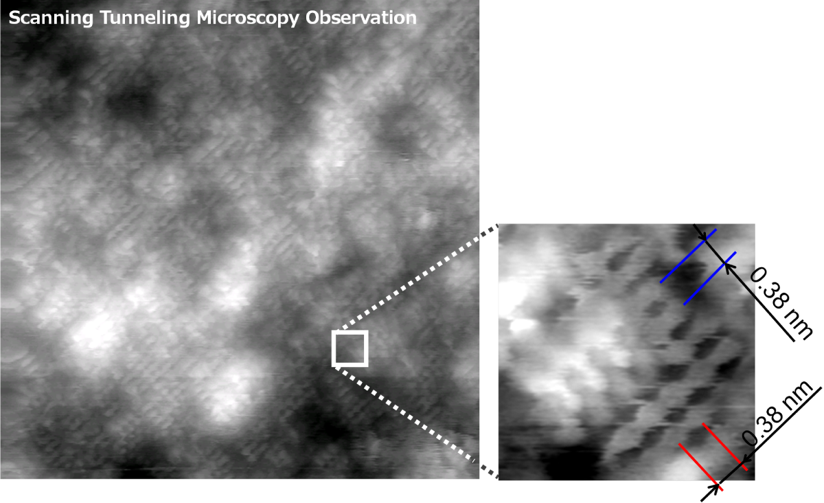

Microscopic understanding of polishing process
Exploration of high-performance nanocarbons for chemical etching
We have been working on the formation of atomic-thick carbon films (graphene) with low pit defect density using a proprietary method that combines plasma treatment on ultra-flat polished silicon carbide (SiC) surfaces. Recently, we have become interested in the corrosive effects exhibited by nanocarbons based on a graphene-like framework. We are currently focused on developing surface creation processes that actively utilize this chemical property.

Selective etching of semiconductor surfaces
by utilizing the corrosive action fo nanocarbons
Development of deep trench/hole machining without mechanical action
Recently, a technique to form deep grooves or holes on semiconductor surfaces in a solution through the catalytic action of noble metals has been gaining attention. Using this technique, elements of different types from the substrate semiconductor can be deeply embedded into the grooves or holes. We adopt a new perspective in which different elements embedded at the bottom are utilized as vertical landmarks. Additionally, we are working on the structural evaluation of the bottom surface of three-dimensional nanostructures with high aspect ratios (depth to width ratio).
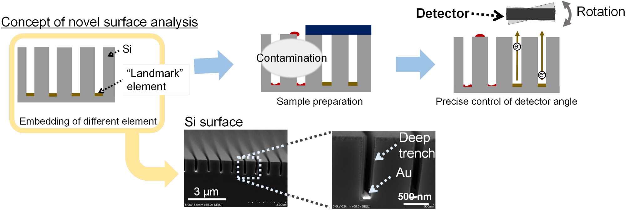
Embedding of Au at bottoms of deep Si trenches
Extreme measurement of wetting properties for electronic devices
In an atmosphere containing water vapor, a thin layer of water (adsorbed water) exists on the surface of all materials. We have been conducting experiments to precisely measure the thickness of adsorbed water on oxides using synchrotron radiation as a probe. Recently, we have developed a unique combined system for surface treatment and measurement to apply the results obtained in this study to the development of next-generation device processes. We believe that this will enable us to systematically investigate the effects of water molecules and volatile organic molecules on the electrical properties of metal-oxide-semiconductor (MOS) structures.

Humidity dependence of adsorbed water layer thickness as measured by synchrotron X-ray photoelectron spectroscopy (XPS)
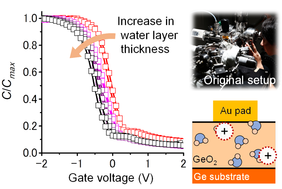
Precise analysis of the effect of adsorbed water on the characteristics of MOS devices
Quantum mechanical computing opening future "manufacturing"
First-principles calculations based on quantum mechanics and potential calculations using machine learning accurately predict the electronic state of solid surfaces and solid-liquid interface phenomena. Combining them with experimental results will contribute to create high-performance nanomaterials and new surface processes.
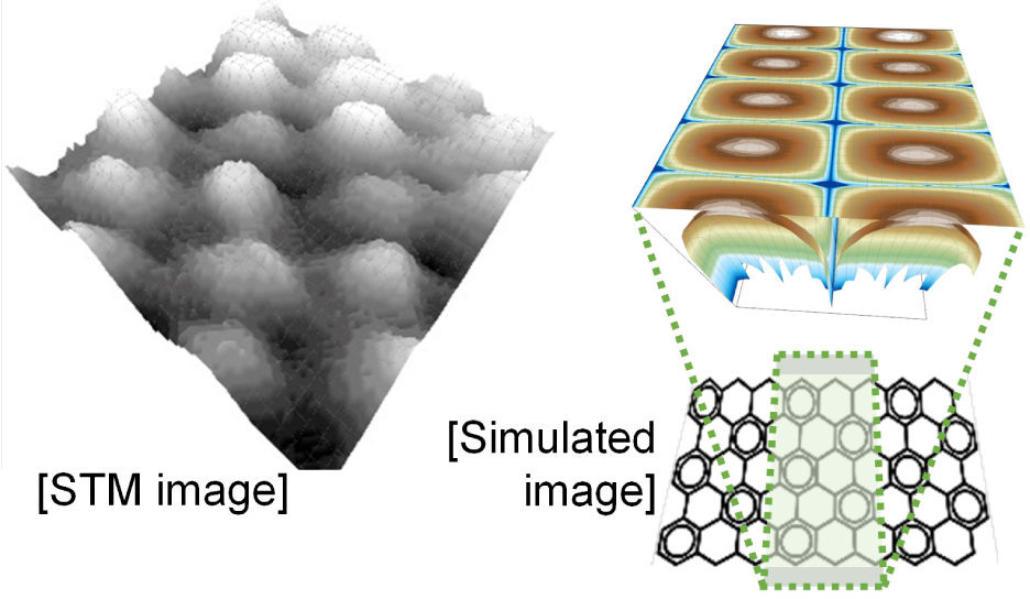
Unique electronic state of
graphene containing linear defects
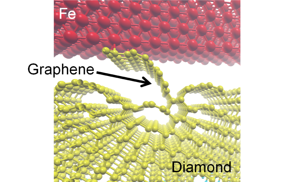
Exfoliation of graphene sheets
at the diamond-iron interface


